- 您现在的位置:买卖IC网 > Sheet目录342 > MCBSTM32EXL (Keil)BOARD EVALUATION FOR STM32F103ZE
�� �
�
�Secure� digital� input/output� interface� (SDIO)�
�RM0008�
�Note:�
�The� DPSM� remains� in� the� Wait_S� state� for� at� least� two� clock� periods� to� meet� the� N� WR� timing�
�requirements,� where� N� WR� is� the� number� of� clock� cycles� between� the� reception� of� the� card�
�response� and� the� start� of� the� data� transfer� from� the� host.�
�●�
�Send:� the� DPSM� starts� sending� data� to� a� card.� Depending� on� the� transfer� mode� bit� in�
�the� data� control� register,� the� data� transfer� mode� can� be� either� block� or� stream:�
�–�
�–�
�In� block� mode,� when� the� data� block� counter� reaches� zero,� the� DPSM� sends� an�
�internally� generated� CRC� code� and� end� bit,� and� moves� to� the� Busy� state.�
�In� stream� mode,� the� DPSM� sends� data� to� a� card� while� the� enable� bit� is� high� and�
�the� data� counter� is� not� zero.� It� then� moves� to� the� Idle� state.�
�If� a� FIFO� underrun� error� occurs,� the� DPSM� sets� the� FIFO� error� flag� and� moves� to� the�
�Idle� state.�
�●�
�Busy:� the� DPSM� waits� for� the� CRC� status� flag:�
�–�
�–�
�If� it� does� not� receive� a� positive� CRC� status,� it� moves� to� the� Idle� state� and� sets� the�
�CRC� fail� status� flag.�
�If� it� receives� a� positive� CRC� status,� it� moves� to� the� Wait_S� state� if� SDIO_D0� is� not�
�low� (the� card� is� not� busy).�
�If� a� timeout� occurs� while� the� DPSM� is� in� the� Busy� state,� it� sets� the� data� timeout� flag� and�
�moves� to� the� Idle� state.�
�The� data� timer� is� enabled� when� the� DPSM� is� in� the� Wait_R� or� Busy� state,� and�
�generates� the� data� timeout� error:�
�–�
�–�
�When� transmitting� data,� the� timeout� occurs� if� the� DPSM� stays� in� the� Busy� state� for�
�longer� than� the� programmed� timeout� period�
�When� receiving� data,� the� timeout� occurs� if� the� end� of� the� data� is� not� true,� and� if� the�
�DPSM� stays� in� the� Wait_R� state� for� longer� than� the� programmed� timeout� period.�
�●�
�Data:� data� can� be� transferred� from� the� card� to� the� host� or� vice� versa.� Data� is�
�transferred� via� the� data� lines� .� They� are� stored� in� a� FIFO� of� 32� words� ,� each� word� is� 32�
�bits� wide.�
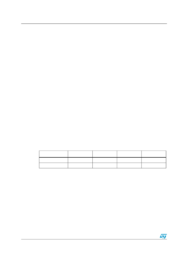
�Table� 125.� Data� token� format�
�Description�
�Block� Data�
�Stream� Data�
�0�
�0�
�Start� bit�
�-�
�-�
�Data�
�yes�
�no�
�CRC16�
�1�
�1�
�End� bit�
�Data� FIFO�
�The� data� FIFO� (first-in-first-out)� subunit� is� a� data� buffer� with� a� transmit� and� receive� unit.�
�The� FIFO� contains� a� 32-bit� wide,� 32-word� deep� data� buffer,� and� transmit� and� receive� logic.�
�Because� the� data� FIFO� operates� in� the� AHB� clock� domain� (HCLK/2),� all� signals� from� the�
�subunits� in� the� SDIO� clock� domain� (SDIOCLK)� are� resynchronized.�
�468/995�
�Doc� ID� 13902� Rev� 9�
�发布紧急采购,3分钟左右您将得到回复。
相关PDF资料
MCBTMPM330
BOARD EVAL TOSHIBA TMPM330 SER
MCIMX25WPDKJ
KIT DEVELOPMENT WINCE IMX25
MCIMX53-START-R
KIT DEVELOPMENT I.MX53
MCM69C432TQ20
IC CAM 1MB 50MHZ 100LQFP
MCP1401T-E/OT
IC MOSFET DRVR INV 500MA SOT23-5
MCP1403T-E/MF
IC MOSFET DRIVER 4.5A DUAL 8DFN
MCP1406-E/SN
IC MOSFET DVR 6A 8SOIC
MCP14628T-E/MF
IC MOSFET DVR 2A SYNC BUCK 8-DFN
相关代理商/技术参数
MCBSTM32EXLU
功能描述:开发板和工具包 - ARM EVAL BOARD + ULINK2 FOR STM32F103ZG
RoHS:否 制造商:Arduino 产品:Development Boards 工具用于评估:ATSAM3X8EA-AU 核心:ARM Cortex M3 接口类型:DAC, ICSP, JTAG, UART, USB 工作电源电压:3.3 V
MCBSTM32EXLU-ED
制造商:ARM Ltd 功能描述:KEIL STM STM32EXL EVAL BOARD
MCBSTM32EXLUME
功能描述:开发板和工具包 - ARM EVAL BOARD + ULINKME FOR STM32F103ZG
RoHS:否 制造商:Arduino 产品:Development Boards 工具用于评估:ATSAM3X8EA-AU 核心:ARM Cortex M3 接口类型:DAC, ICSP, JTAG, UART, USB 工作电源电压:3.3 V
MCBSTM32F200
功能描述:开发板和工具包 - ARM EVAL BOARD FOR STM STM32F207IG
RoHS:否 制造商:Arduino 产品:Development Boards 工具用于评估:ATSAM3X8EA-AU 核心:ARM Cortex M3 接口类型:DAC, ICSP, JTAG, UART, USB 工作电源电压:3.3 V
MCBSTM32F200U
功能描述:开发板和工具包 - ARM EVAL BOARD FOR STM STM32F207IG + ULINK2
RoHS:否 制造商:Arduino 产品:Development Boards 工具用于评估:ATSAM3X8EA-AU 核心:ARM Cortex M3 接口类型:DAC, ICSP, JTAG, UART, USB 工作电源电压:3.3 V
MCBSTM32F200UME
功能描述:开发板和工具包 - ARM EVAL BOARD FOR STM STM32F207IG ULINK-ME
RoHS:否 制造商:Arduino 产品:Development Boards 工具用于评估:ATSAM3X8EA-AU 核心:ARM Cortex M3 接口类型:DAC, ICSP, JTAG, UART, USB 工作电源电压:3.3 V
MCBSTM32F200UME-ED
制造商:ARM Ltd 功能描述:KEIL STM32F207IG EVAL BOARD
MCBSTM32F400
功能描述:开发板和工具包 - ARM EVAL BOARD FOR STM STM32F407IG
RoHS:否 制造商:Arduino 产品:Development Boards 工具用于评估:ATSAM3X8EA-AU 核心:ARM Cortex M3 接口类型:DAC, ICSP, JTAG, UART, USB 工作电源电压:3.3 V